 2026/08/07
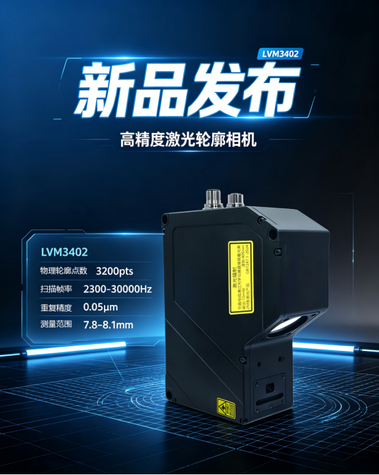
Semiconductor packaging, optical modules, and 3C precision manufacturing—what do these industries have in common? The workpieces are becoming increasingly smaller, the tolerances are becoming tighter, and handling reflective surfaces is becoming more challenging.
A chip the size of a fingernail, a highly reflective surface plated with gold and nickel, and micron-level tolerance requirements. When scanned by a general-purpose line laser camera, bright areas appear as blindingly white, while dark areas result in lost data, and spot detection becomes highly erratic. Traditional inspection methods either lack sufficient precision, fail to keep up with processing speeds, or completely fail when encountering highly reflective surfaces.
YiShi Technology has newly launched the LVM3402 industrial-grade ultra-precision 3D line laser camera, specifically designed for applications characterized by "small size, high reflectivity, and micron-level tolerances."
A set of parameters to understand the hardware capabilities of the LVM3402
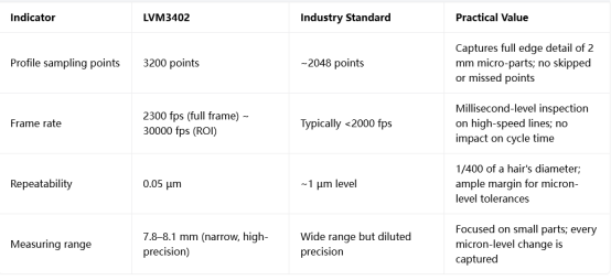
It goes beyond simply piling up parameters; it represents a systemic enhancement of underlying capabilities.
The LVM3402 belongs to the LVM3000 series platform launched by Next Vision Tech in 2025. This series represents more than a simple product iteration; rather, it is a "platform-based product" designed for the intelligent manufacturing ecosystem—featuring end-to-end in-house development of optical solutions and imaging algorithms, leveraging FPGA-based real-time processing to complete algorithms within a single frame scan, thereby enabling high-speed, high-performance measurement capabilities.
Hardware: folded optical path—compact design, powerful performance
The all-new optical path system employs a foldable optical path architecture tailored for small-field-of-view scenarios, significantly reducing camera footprint while greatly enhancing installation flexibility. This compact design can be easily integrated into existing equipment, eliminating the need for modifications to current production lines. The reduced single-point sampling pitch and improved Z-axis resolution provide the physical foundation for a repeatability precision of 0.05 μm.
Algorithmic level: Intelligent HDR fusion for unified exposure of bright and dark areas within the same frame
Our proprietary multi-material HDR fusion algorithm goes beyond simple frame averaging; instead, it intelligently identifies the reflective characteristics of different materials and dynamically adjusts the exposure strategy—effectively suppressing highlights in bright areas while enhancing weak signals in dim areas. As a result, the point cloud maintains well-defined bright regions without blown-out whites, and preserves dark regions without point loss, ensuring complete and continuous contours free of flying points or image discontinuities. What was once deemed "impossible to measure" is now easily controllable.
Deployment level: standardized dimensions, plug-and-play
The LVM3402 shares the same mechanical mounting dimensions as other models in the LVM3000 series, eliminating the need for redesigning fixtures. When paired with a dedicated junction box, complex cables are simplified to standard interfaces, significantly reducing deployment time and maintenance costs.
Classic Scenario: The "killer" of 0.018 mm solder joints for 2 mm semiconductor chip pins
Pain point: While incoming material inspection yields "pass" results, the solder joint failure rate surges after placement on the chip mounting machine—actual pin height exceeds the substrate by 0.018 mm, with a deviation of only 3 μm; however, traditional cameras suffer from insufficient sampling, reflective artifacts, and inaccurate measurements.
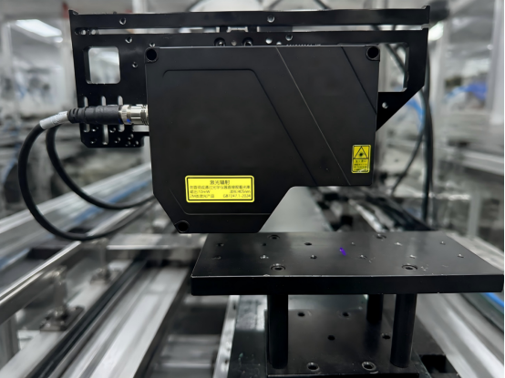
Solution (LVM3402)
·HDR multi-frame compositing ensures seamless integration of metallic and black materials within the same frame.
·3,200 points + narrow range; 100% capture of edge details
· Measured Z-axis repeatability ≤ 0.0005 mm (customer requirement: 0.0006 mm); 100% of pins exhibit valid data; continuous absence of breaks on the black substrate
· Single-piece inspection time <50 ms; online full inspection detects and rejects defective parts, significantly reducing scrap losses after component mounting.
This applies not only to chip pins, but also to these other scenarios.
The stable imaging capability in scenarios featuring the coexistence of high-and low-reflectivity surfaces ensures that the LVM3402 is not only suitable for semiconductor packaging inspection:
✅ Optical Communication: Planarity of optical module base and height difference of LPO module
✅ 3C Precision Manufacturing: Smartphone frame step variation and camera mount coplanarity
✅ Semiconductors: Planearity of lead frames, warpage of packaging substrates
✅ New Energy: Planarity of IGBT heat dissipation substrate and height of cell connection tabs
If your workpieces also require inspection under conditions featuring the coexistence of "metal reflective parts and black light-absorbing parts," small dimensions, and micron-level tolerances, please contact us. We can provide free sample inspections for your workpieces and develop customized visual inspection solutions tailored to your specific needs.


 浙公网安备33021202004092号