 2026/09/18
Industry Pain Points in Online Memory Module Measurement
A memory module is not a "uniform surface." Instead, its surface is a mixture of three distinct reflective properties:
·PCB surface: dark solder mask layer, high light absorption, low reflectivity
· Chip encapsulation package: uneven reflectivity and irregular micro-texture on the surface
·Gold Finger: Hard gold plating with high reflectivity, featuring an extremely narrow active area that alternates with low-reflectivity zones.
In the case of such surfaces, conventional laser processing schemes may encounter several chain reactions:
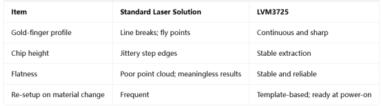
Golden Finger focus issues: high reflectivity leading to overexposure, weak reflectivity in gaps, and broken contours.
Chip height jump: significant difference in reflectivity between the plastic package and the PCB, resulting in unstable edge positioning.
Flatness distortion: poor point cloud quality, rendering feature extraction meaningless
Adjust parameters whenever the batch changes: each new batch requires reconfiguration, and the production line must wait.
Inaccurate flatness measurement has never been an algorithmic issue; it is fundamentally a point cloud issue. If the point cloud is unclean, the subsequent results will be nothing more than a house of cards.
Customer requirements: chip height, chip flatness, and gold finger flatness—each of these three parameters must be ≤3 μm—and the process must deliver consistent and stable output continuously throughout the production line cycle time.
Deliverable, verifiable results
-The transition between the chip surface and the PCB edge is sharp, the gold fingers exhibit well-defined edges, and there are no broken lines or stray dots.
-The chip exhibits a peak fluctuation of approximately 2.3 μm.
-Flatness evaluation of the chip top surface: approximately 2 μm
-Flatness evaluation of the gold finger: approximately 2.8 μm
All three criteria are met, and the performance is not merely "occasional compliance"; rather, it represents stable output achieved through continuous operation on the production line after optimization, without the need for frequent parameter adjustments.

Fundamental technical principles of stable measurement
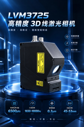
01 High-density physical contour acquisition
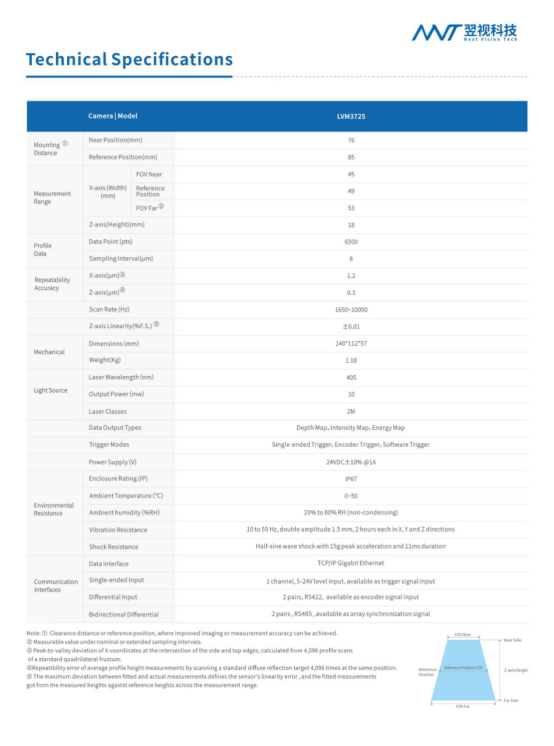
6,500 pts: physical contour points that provide high-density coverage of detailed areas—such as chip edges and lead gap regions—ensuring no missed points at steps or boundaries.
02 High-frame-rate dynamic scanning
With a scan frame rate ranging from 1,650 to 10,000 Hz, the system is tuned to match the motion speed of the production line, ensuring complete contour integrity and the absence of motion blur or line breaks even during high-speed passage.
03 Optical Path and Exposure Optimization
To optimize the imaging pipeline for mixed reflective surfaces—including dark solder mask on PCBs, chip plastic encapsulation, and gold fingers—this approach suppresses overexposure and loss of detection points due to weak reflectivity, thereby yielding cleaner and more complete point clouds at the underlying level.
04 Micron-level repeatability
With a repeatability of 0.3 μm, this provides reliable foundational data for the consistent extraction of chip height, chip flatness, and gold finger flatness.
Point Cloud Imaging: Real-World Imaging and Quality Assessment
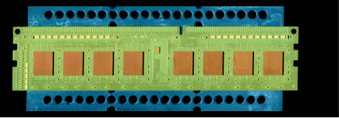
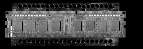
Based on real-world 3D point clouds (top: pseudo-color image / right: brightness map)
The transition between the chip's top surface and the PCB edge is sharp, and the edges of the gold fingers are well-defined, free of broken lines or stray spots. This high-quality underlying point cloud ensures that the extraction of the chip height, chip planarity, and gold finger planarity is stable and reliable.
Comparison with measured results under comparable operating conditions
This applies not only to memory modules, but also to these other scenarios.
✅ Measurement of memory module chip height, chip flatness, and gold fingers flatness
✅ Materials with complex surface textures and significant color variations
✅ In-line dimensional and flatness inspection for high-speed production lines
✅ Industrial measurement requiring micron-level repeatability precision
From delivery to service—we take full responsibility.
Selecting the right equipment is not just about choosing a camera.
· Free sample testing: Submit sample → Receive point cloud data and measurement report within 48 hours → Select appropriate model once compliance is confirmed
· Ready-to-use: Provides parameter templates based on material type, reducing on-site parameter tuning time.
· Integrated Support: SDK, calibration, algorithm parameters, and communication protocol integration support
· After-sales support: dedicated FAE technical team support; provision of backup equipment for emergency services
Our goal is not to sell you the camera, but to ensure that your detection workstation runs stably.
Hardware Technical Specifications
If your workpieces also face challenges such as "complex surface geometries, significant color variations, and micron-level inspection on high-speed production lines":
① Contact Us → ② Request Samples for Free Testing → ③ Access Test Reports → ④ Customize Visual Inspection Solutions
We offer free sample testing and customized solutions, using your materials and your specific operating conditions to validate performance—rather than relying solely on technical datasheets.


 浙公网安备33021202004092号